Best PCB Design Course at Tech Booster.
PCB Designing in Guwahati!!!
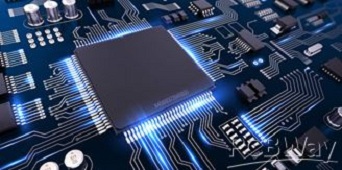
Tech Booster, Guwahati's best institute for PCB designing course provides you the best of trainings from the best of trainers. PCB designing course is a computer-aided designing technology. It is used to plan and design circuit boards for electronics circuits designed to deliver a specific output or outputs. PCB designing is browned for both through-hole and surface mount electronic components. (PCB) Printed circuit board design brings your electronic circuits to life in the physical form. Utilizing layout software, the PCB design process combines component placement and routing to define electrical connectivity on a manufactured circuit board.It is a laminated sandwich structure of conductive and insulating layers. PCBs mechanically support electronic components using conductive pads in the shape designed to accept the component's terminals, and also electrically connect them using traces, planes and other features etched from one or more sheet layers of copper laminated onto and/or between sheet layers of a non-conductive substrate.
Characteristics of PCB Designing:
Through-hole technology,
Surface-mount technology,
Circuit properties of the PCB,
Materials